Beneath the Chip: How a New Wave of American Startups Is Fortifying the Semiconductor Supply Chain

When most Americans think about semiconductor independence, they picture sprawling fabrication plants rising from desert landscapes in Arizona or the plains of Ohio. Those facilities are real, consequential, and enormously expensive. But the executives, engineers, and investors who work most closely with the semiconductor industry will tell you something that rarely surfaces in policy briefings or earnings calls: a fabrication plant is only as strong as the supply chain feeding it.
That supply chain — stretching from ultra-pure specialty gases and advanced photoresist chemicals to chip packaging substrates, electronic design automation software, and precision testing equipment — remains deeply fragmented, heavily reliant on suppliers concentrated in Japan, South Korea, Taiwan, and the Netherlands, and largely invisible to the general public. It is precisely this invisible infrastructure that a new generation of American startups has set out to rebuild.
The Layers Nobody Talks About
Semiconductor manufacturing is not a single process. It is a cascade of highly specialized operations, each dependent on inputs that must meet tolerances measured in nanometers or parts per billion. Before a single transistor is etched onto a wafer, manufacturers require chemical mechanical planarization slurries, photolithography-grade solvents, and dielectric materials engineered to exacting specifications. After fabrication, chips must be packaged — a process that has grown dramatically more complex as the industry moves toward chiplet architectures and three-dimensional integration.
Then there is the matter of verification. Every chip must be tested before it ships, and the equipment used to perform that testing represents its own specialized industrial segment. So does the software used to design chips in the first place; electronic design automation tools, long dominated by a handful of established vendors, are now being challenged by startups deploying artificial intelligence to compress design cycles and reduce engineering overhead.
Each of these layers represents a potential chokepoint. And each, until recently, was treated as someone else's problem.
Specialty Materials: Closing the Chemistry Gap
Among the most consequential areas of startup activity is the domestic production of semiconductor-grade specialty materials. The United States currently imports a significant share of the high-purity chemicals and advanced substrates required for leading-edge fabrication. Companies such as Entegris have long served this market, but a newer cohort of ventures is targeting specific gaps with greater precision.
Several early-stage firms are developing domestic sources of advanced photoresists — the light-sensitive polymers central to lithographic patterning — while others are focused on silicon carbide and gallium nitride substrates critical to power semiconductors used in electric vehicles and defense systems. The strategic logic is straightforward: if a single foreign supplier of a niche precursor chemical faces disruption, the consequences can ripple across an entire manufacturing ecosystem within weeks.
Investors have taken note. Venture capital flowing into semiconductor materials startups has increased meaningfully since 2022, accelerated in part by CHIPS and Science Act incentives that have made the sector considerably more attractive to institutional capital.
Advanced Packaging: Where the Next Performance Gains Live
For decades, the semiconductor industry's primary performance lever was shrinking transistors. As that approach encounters physical limits, advanced packaging — the art of combining multiple chips or chiplets into a single, tightly integrated module — has emerged as the new frontier of performance engineering.
This shift has opened significant opportunity for American startups. Companies working on heterogeneous integration, fan-out wafer-level packaging, and silicon photonics interconnects are attracting both venture funding and strategic interest from defense contractors and hyperscale cloud providers. The argument for domestic capability here is not merely economic; advanced packaging for military and intelligence applications carries obvious national security implications that make foreign dependency particularly untenable.
Startups in this space are also benefiting from proximity to U.S. research institutions. DARPA's Electronics Resurgence Initiative and programs run through the National Science Foundation have seeded academic work that several packaging-focused ventures have successfully commercialized.
Design Software: AI Enters the EDA Arena
Electronic design automation has historically been a market of remarkable concentration. A small number of established players have dominated the tools that chip designers use to translate concepts into manufacturable layouts. That concentration, combined with the growing complexity of modern chip architectures, has created a genuine opening for AI-native challengers.
Several American startups are now deploying machine learning to automate portions of the chip design process that previously required months of skilled engineering labor. Tasks such as floorplanning, timing closure, and physical verification — once painstaking manual endeavors — are being accelerated by generative and reinforcement learning models trained on vast libraries of prior design data.
The implications extend beyond efficiency. Faster design cycles lower the barrier to entry for specialized chip development, enabling defense primes, automotive manufacturers, and industrial technology companies to pursue custom silicon that would previously have been cost-prohibitive. In a world where competitive advantage increasingly flows from hardware differentiation, accessible design tooling is a genuine force multiplier.
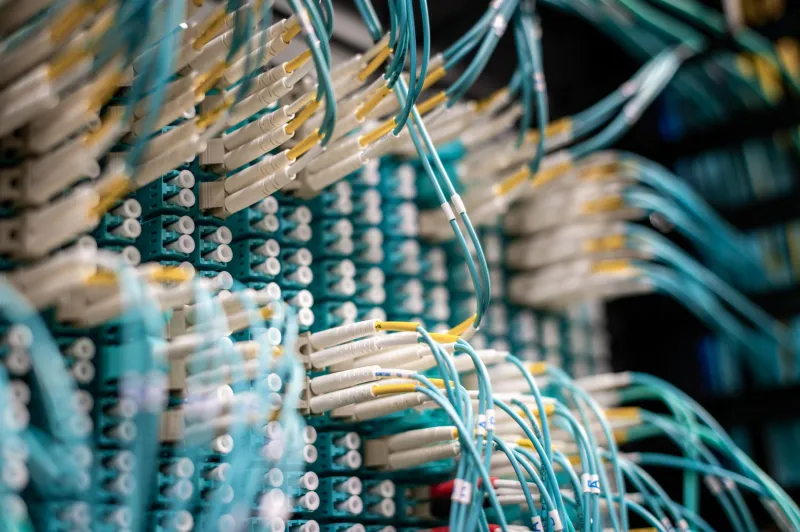
Testing and Verification: The Final Frontier
No chip reaches a customer without passing through a battery of functional and parametric tests. Automated test equipment represents a capital-intensive, technically demanding segment historically dominated by a small group of Japanese and American incumbents. But the transition to chiplet-based architectures and the proliferation of AI accelerators have introduced testing challenges that legacy equipment was not designed to address.
A handful of startups are developing test platforms purpose-built for these emerging device classes, combining novel probe technologies with software-defined test architectures that can adapt more rapidly to new chip designs. Some are also targeting the inspection and metrology equipment used during fabrication itself — tools that detect defects at the atomic scale and that currently depend heavily on European and Asian suppliers.
What 2030 Could Look Like
Policymakers in Washington have begun to recognize that funding fabrication plants without attending to the surrounding supply ecosystem is an incomplete strategy. Recent CHIPS Act implementation guidance has expanded its focus to include upstream materials and downstream packaging, and several national laboratories have launched programs specifically targeting supply chain gaps identified through industry consultation.
If current investment trajectories hold and regulatory frameworks continue to incentivize domestic sourcing, a meaningfully different landscape could take shape by the end of the decade. It would not be a fully self-contained American semiconductor ecosystem — global interdependence is both inevitable and, in many respects, desirable. But it would be one in which the United States holds defensible positions across a far broader range of critical supply chain nodes than it does today.
The startups building toward that future are, for now, operating largely outside public view. Their names do not appear on the facades of the fabrication plants that draw governors to ribbon-cutting ceremonies. But the chips that emerge from those plants — and the national security and economic competitiveness that depend on them — will ultimately rest on the foundations these companies are quietly laying.
The visible infrastructure of American semiconductor ambition is impressive. The invisible infrastructure being constructed beneath it may prove to be the more important story.