Chips Down: The Quiet American Buildout Underneath the AI Revolution
Every conversation about artificial intelligence eventually arrives at the same inconvenient truth: models run on silicon, and America does not make nearly enough of it at home. While policymakers debate export controls and tech executives unveil ever-larger language models, a less celebrated cohort of engineers and entrepreneurs is doing something considerably more concrete. They are constructing, piece by painstaking piece, a domestic semiconductor supply chain capable of sustaining the country's AI aspirations without depending on fabrication facilities thousands of miles away.
This is not a story about Nvidia's latest GPU announcement or the next frontier model from a San Francisco laboratory. It is a story about the layer beneath all of that — the fabs, the packaging firms, the electronic design automation toolmakers, and the logistics networks that transform raw wafers into the processors powering American industry. It is, in short, a story about infrastructure, and the startups quietly engineering it.
A Structural Vulnerability Years in the Making
The United States once dominated every segment of semiconductor manufacturing. That dominance eroded steadily over several decades as production migrated to East Asia, drawn by lower labor costs, generous government subsidies, and the singular manufacturing expertise that Taiwan Semiconductor Manufacturing Company — TSMC — accumulated over a generation. By the early 2020s, the US accounted for roughly 12 percent of global chip production, down from nearly 37 percent in 1990.
The passage of the CHIPS and Science Act in 2022 injected approximately $52 billion into domestic semiconductor manufacturing and research, signaling a bipartisan recognition that the vulnerability was real. But federal appropriations, however substantial, do not by themselves create the dense ecosystem of suppliers, designers, and process engineers that a mature semiconductor industry requires. That ecosystem must be grown. And increasingly, startups are doing the growing.
The Architecture Insurgents
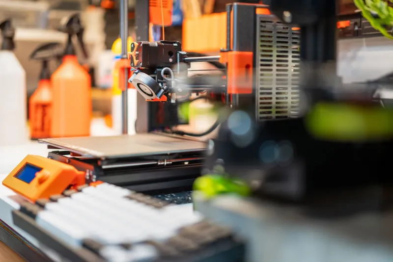
In Austin, Texas, a cluster of chip design firms has coalesced around RISC-V, an open-source instruction set architecture that offers an alternative to the proprietary designs that have long defined the industry. Unlike the licensing-dependent architectures that dominated the previous decade, RISC-V allows companies to design custom processors without paying royalties to a single gatekeeper — a structural advantage that has attracted significant startup activity.
Firms operating in this space are targeting everything from edge AI inference chips to domain-specific accelerators built for particular industrial workloads. The appeal is straightforward: custom silicon tailored to a specific application can deliver dramatic efficiency gains over general-purpose processors. For a manufacturing plant running continuous machine vision or a hospital network processing medical imaging data, those efficiency gains translate directly into operating cost reductions.
The architectural openness of RISC-V also reduces geopolitical exposure. A design built on an open standard is harder to sanction, harder to restrict, and easier to replicate across multiple foundries — a consideration that has grown considerably more relevant as US-China technology tensions have intensified.
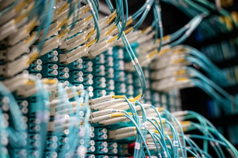
Packaging: The Overlooked Bottleneck
If chip design is the discipline that attracts the most startup attention, advanced packaging is the one that arguably carries the most strategic weight right now. Packaging — the process of integrating multiple chips into a single assembly, connecting them with high-speed interconnects, and preparing them for deployment — has become a critical differentiator in AI hardware performance.
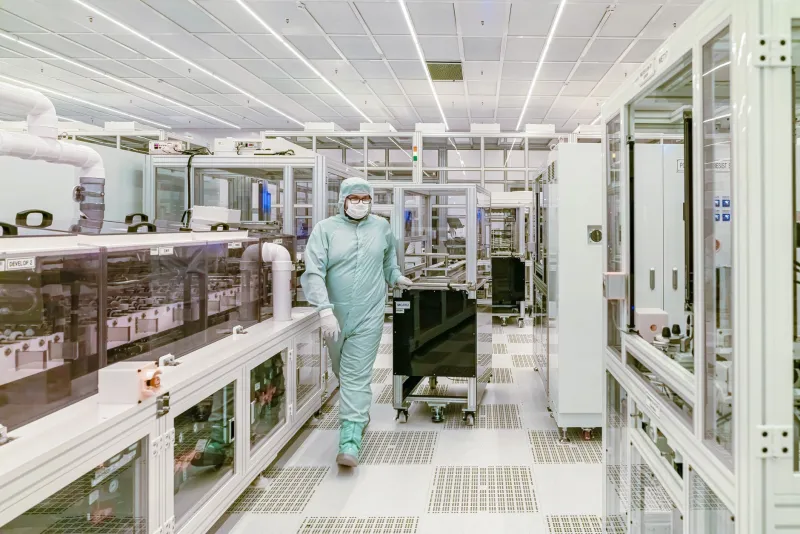
Arizona has emerged as a meaningful hub for this segment of the supply chain. Intel's investment in its Chandler fabrication complex brought advanced packaging capabilities to the region, and a supporting ecosystem of smaller firms has followed. Several startups are now developing chiplet integration technologies and heterogeneous packaging solutions designed to allow chips from different manufacturers and process nodes to work together efficiently.
This matters enormously for AI workloads. The memory bandwidth and interconnect density required by large-scale AI training and inference push conventional packaging approaches to their limits. Startups that can deliver credible next-generation packaging solutions are addressing a genuine engineering constraint, not a speculative future need.
Venture Capital Recalibrates
For much of the past decade, semiconductor startups occupied an uncomfortable position in the venture capital landscape. The capital requirements were high, the development timelines were long, and the exit multiples rarely matched those available in software. Many investors simply passed.
That calculus has shifted. The combination of the CHIPS Act's incentive structures, the AI industry's voracious appetite for specialized silicon, and a clearer understanding of the strategic stakes involved has drawn a new wave of investment into the sector. Several dedicated semiconductor-focused funds have launched in recent years, and generalist firms that previously avoided hardware have begun making selective exceptions for companies operating at the intersection of AI and chip design.
The investment thesis is no longer purely financial. National security considerations, supply chain resilience, and the strategic importance of maintaining domestic semiconductor expertise have all become legitimate parts of the conversation between founders and their backers. That shift in framing has opened doors that were previously closed.
The Workforce Equation
Capital is necessary but not sufficient. Semiconductor engineering requires highly specialized human expertise — process engineers, materials scientists, electronic design automation specialists — and that expertise takes years to develop. One of the less-discussed challenges facing the domestic buildout is a workforce pipeline that has not kept pace with the industry's ambitions.
Several startups have responded by partnering directly with universities, establishing apprenticeship programs, or recruiting internationally and sponsoring visa applications for engineers who want to build their careers in the United States. Community colleges in states with significant fab investment, including Arizona, Ohio, and New York, have begun developing technical programs designed to feed the manufacturing workforce that new facilities will require.
This is slow, deliberate work. It does not generate press releases or venture announcements. But it may ultimately prove as consequential as any individual product breakthrough.
Building Without the Spotlight
There is a particular kind of startup founder who is drawn to problems that are genuinely difficult, structurally important, and largely invisible to the general public. The entrepreneurs building the American semiconductor supply chain tend to fit that description. They are not chasing the cultural cachet that attaches to consumer applications or social platforms. They are solving engineering problems that have geopolitical consequences.
The work is unglamorous by design. Fab processes are measured in nanometers and yield rates. Packaging innovations are expressed in microbump densities and thermal dissipation figures. These are not metrics that trend on social media. But they are the metrics that determine whether the United States can sustain an AI industry that does not depend on the continued goodwill of foreign governments and the uninterrupted operation of facilities on the other side of the Pacific.
Washington has articulated the goal. The startups, engineers, and investors working across Austin, Phoenix, Columbus, and Albany are doing the considerably harder work of actually achieving it — one wafer, one design tape-out, and one packaging innovation at a time.